This is not an incremental spec bump. The T100 collapses what used to be multi-tier switching fabrics into flatter, higher-radix topologies, eliminating entire layers of infrastructure that hyperscalers have been forced to build around the bandwidth ceilings of prior-generation silicon. The implications ripple from data center architecture down to rack power budgets and capital expenditure plans.
Why Network Bandwidth Became an AI Problem
When GPU clusters were measured in hundreds of cards, conventional Ethernet fabrics could keep pace. Scale to tens of thousands of accelerators — the baseline for frontier model training today — and the arithmetic changes fundamentally. Collective communication operations like AllReduce, which synchronize gradients across every GPU in a training run, saturate whatever bandwidth the network can provide. A faster GPU without a faster interconnect simply idles more.
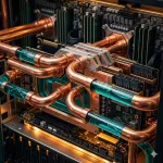
The rack power dimension compounds the problem. Modern AI racks approach 120 kW of power consumption. Network components — switches, transceivers, cables — already consume 15 to 25 percent of total rack power in dense GPU deployments. Every watt saved in the switching layer is a watt available for compute, or a watt that does not need to be provisioned in cooling infrastructure.
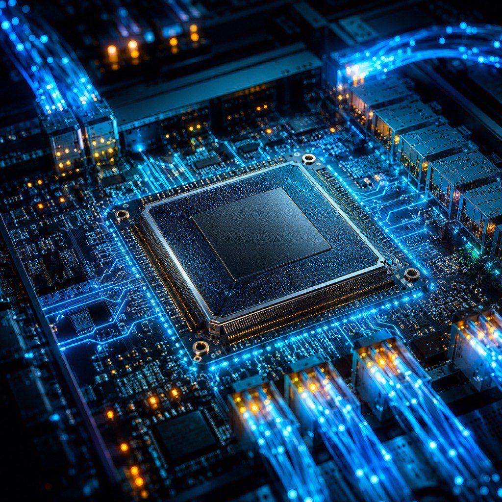
Prior-generation switch silicon, including competing solutions at lower bandwidth tiers, carried architectural decisions made for general-purpose cloud traffic — decisions that added power and die area without benefiting AI workloads. The Teralynx T100 was designed without that legacy, using a monolithic die on 3nm to deliver 102.4 Tbps under a 1,000-watt typical power envelope.
What 102.4 Tbps on 3nm Actually Means
The headline number — 102.4 Tbps aggregate bandwidth — is eight times the 12.8 Tbps entry point of the Teralynx product family and roughly double what the previous generation of high-end switch silicon offered at scale. Achieveing this on a single monolithic die, rather than through chiplet aggregation, matters for latency: inter-die communication overhead is eliminated, and the switching decision path stays entirely on one piece of silicon.
The 3nm process node is where much of the power efficiency gain originates. Smaller transistors switch faster at lower voltages, and Marvell’s advanced low-power SerDes architecture — the high-speed serial links that carry data on and off the chip — benefits directly from the node shrink. The result is up to 25 percent lower power consumption compared with competitive solutions at comparable bandwidth tiers.
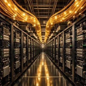
Port flexibility is a key architectural lever. The T100 supports up to 512-port radix configurations, which means a single switch can connect hundreds of servers or GPU nodes directly without an intermediate aggregation layer. In traditional three-tier (access / aggregation / core) data center designs, eliminating one tier removes both capital cost and an additional hop of latency on every packet that crosses fabric boundaries.
Three package configurations address different deployment scenarios. Ball grid array (BGA) is the conventional approach, suitable for standard PCB assembly. Co-packaged copper (CPC) tightens the electrical connection between the ASIC and copper cable assemblies, reducing signal loss at very high data rates. Co-packaged optics (CPO) integrates optical transceivers directly with the switch die, eliminating the pluggable module entirely and cutting optical interconnect power by a significant margin — a critical option as data center operators plan for 800G and 1.6T port speeds.
Protocol support is aligned with the emerging AI networking stack. The T100 implements Ethernet Scale-Up Networking (ESUN) and meets Ultra Ethernet Consortium (UEC) requirements, both of which are designed to give Ethernet the low-latency, lossless behaviour historically associated with InfiniBand — the incumbent interconnect for AI supercomputers. Software integration covers Marvell’s SDK, the Open Compute Project Switch Abstraction Interface (SAI), and the SONiC network operating system, giving operators a path to deploy the hardware within existing open-networking automation stacks.
Advertisement
The Competitive Landscape: Chasing Broadcom and Cisco
Marvell does not operate in a vacuum. Broadcom’s Tomahawk series has dominated merchant switch silicon for over a decade, and the Tomahawk 5 — operating at 51.2 Tbps — set the previous high-water mark for production-ready switching bandwidth. The T100’s 102.4 Tbps doubles that figure and does so on a newer process node.
Cisco’s Silicon One architecture, developed for Cisco’s own routing and switching products but also licensed to third-party system builders, competes at the high end with latency and programmability as differentiators. Intel’s Tofino, now under different ownership, targets the programmable-pipeline niche. None of these alternatives currently offer a merchant silicon product at 102.4 Tbps.
The “purpose-built for AI” positioning is a direct shot at the legacy architectural decisions baked into general-purpose switch ASICs. Features like AI-native congestion control and integrated telemetry — which surfaces real-time utilisation and flow-level statistics — are increasingly necessary as operators try to maximise GPU utilisation in training clusters where a single congestion event can stall thousands of accelerators simultaneously.
Hyperscalers with custom silicon programmes (Google’s Jupiter series, Meta’s Wedge, Amazon’s Annapurna-derived switching ASICs) represent a different competitive axis. These companies design their own networking hardware for maximum workload specificity. The T100 competes for the same deployments at cloud providers and AI-focused infrastructure operators who prefer merchant silicon over the significant engineering investment required to develop custom ASICs.
What Infrastructure Architects and Operators Should Do
1. Audit Current Fabric Power Budgets Against AI Workload Projections
Before the next refresh cycle, map the percentage of rack power consumed by switching infrastructure today and model what that figure becomes as GPU density increases. If network components already consume 20 percent or more of rack power, the 25 percent efficiency improvement from the T100 materially changes the total cost of ownership calculation — both in direct power spend and in the cooling infrastructure required to manage heat dissipation. Quantify the gap now, while procurement timelines still allow for design changes.
2. Evaluate Topology Simplification as a First-Order Design Goal
The 512-port radix of the T100 makes two-tier (spine-leaf without separate aggregation) and even single-tier flat fabrics viable at scales that previously required three tiers. Model the topology options for your target cluster size: fewer tiers means fewer switch hops, lower east-west latency, fewer optical transceivers or cable assemblies, and simplified network management. The capital and operational savings from eliminating a switching tier can be substantial — and the T100’s high-radix design is specifically architected to enable this simplification.
3. Plan Co-Packaged Optics Adoption into the Infrastructure Roadmap
CPO integration is not a niche option — it is the packaging direction that 800G and 1.6T deployments are converging on as pluggable transceiver power and cost become prohibitive at very high port densities. The T100’s CPO support positions it for this transition. Infrastructure teams should begin engaging system integrators and ODMs now about CPO-based switch platforms, assess cabling plant implications (CPO requires factory-terminated assemblies rather than field-pluggable modules), and include CPO qualification timelines in the roadmap for any new build that will run past 2027.
The Bigger Picture: Ethernet Closing the Gap on InfiniBand
The Teralynx T100 arrives at a moment when Ethernet and InfiniBand are in genuine competition for AI cluster interconnects for the first time in years. NVIDIA’s NVLink and InfiniBand have dominated the highest-performance AI supercomputer designs, but the economics of scale and the universal availability of Ethernet tooling give Ethernet a structural advantage in large cloud deployments.
The UEC and ESUN protocol enhancements that the T100 supports are the technical bridge that closes the remaining behavioural gap. Lossless forwarding, sub-microsecond latency under load, and adaptive routing — once the exclusive domain of InfiniBand — are now achievable on standard Ethernet hardware. If the T100 samples successfully and reaches production at scale in late 2026, it will accelerate the displacement of proprietary interconnects in the hyperscaler AI infrastructure that trains the models used by hundreds of millions of people.
The 3nm process node also signals a broader trend: the same silicon miniaturisation that drove CPU and GPU performance for decades is now being applied specifically to networking silicon. The result is switch ASICs that are not incrementally faster versions of their predecessors but qualitatively different devices — purpose-shaped for the AI workloads that now define data center design.
Frequently Asked Questions
Q: How does the Teralynx T100 differ from standard data center switches?
Standard Ethernet switches are designed for general-purpose east-west and north-south cloud traffic. The T100 is purpose-built for AI training and inference workloads: its congestion control is tuned for the bursty, synchronised collective communication patterns that GPU training generates, its telemetry is designed to surface GPU utilisation impact from network events, and its 512-port radix enables flatter topologies that reduce latency hops between accelerators. The 3nm process node and clean-sheet architecture also strip out power overhead carried by general-purpose switch ASICs for features that AI workloads do not use.
Q: When will the Teralynx T100 be available in production systems?
Marvell began sampling the T100 to customers in Q2 2026 (announced June 1, 2026). Production silicon sampling is typically followed by a 6 to 12 month integration period during which system vendors build T100-based switch platforms and qualify them. Production deployments at hyperscalers are therefore most likely in the H2 2026 to H1 2027 window, depending on customer integration timelines.
Q: What is co-packaged optics and why does it matter for AI switches?
Co-packaged optics (CPO) integrates optical transceiver components directly onto the switch package alongside the ASIC, replacing the pluggable QSFP modules that connect switch ports to fiber cables in conventional designs. At port speeds of 800G and above, pluggable modules consume substantial power and introduce signal integrity challenges. CPO eliminates the electrical interface between the chip and the transceiver, cutting optical component power significantly and enabling denser, higher-speed port configurations. For AI switches handling hundreds of 800G or 1.6T links, CPO is expected to become the dominant packaging approach.
Sources & Further Reading
- Further Reading
- Marvell Announces 102.4 Tbps AI Cloud Data Center Switch — Marvell Newsroom
- Marvell Announces Availability of Industry’s First 102.4 Tbps Switch Purpose-Built for AI — Marvell Investor Relations
- Marvell Unveils 102.4 Tbps AI Switch — Advanced Packaging News
- Marvell Announces Availability of Industry’s First 102.4 Tbps Switch — Investing News Network
🔗 Related Intelligence
Anthropic’s TPU Partnership: Gigawatts of AI Compute Coming in 2027

AI Data Centers: The Architecture Behind the AI Revolution
The Hidden Bottleneck Halting the AI Data Center Boom: Transformer and Switchgear Shortages

Google TPU 8t/8i: The Dual-Chip Architecture Reshaping Enterprise AI Compute in 2026